Octek 286 Motherboard Review - Part 1
In September 2014, I picked up a bundle from EBay for £48, which consisted of this Octek 80286 motherboard with CPU, an IBM 5x86 CPU, memory, MFM disk controllers, video cards, floppy and CD-ROM drives and a few other bits. This Baby AT motherboard was what I was really interested in checking out, and here it is:
What is immediately obvious is the corrosion in the lower right corner, caused by the now missing coin cell CMOS backup battery. The board has few identifying marks on the silkscreen to indicate its manufacturer or model number - the company logo is actually Octek, and it's a Rev 2.1 board - later during boot-up it displays DCS-286, so there we have it - an Octek DCS-286. Searching through Stason.org and other online searches came up blank for this board layout.
Quick Visual Inspection
Looking around the board it appears to consist of the following:
- A socketed Intel 80286-10.
- G2 chipset (Headland Technologies), consisting of 3 chips.
- A socket for an 80287 math co-processor.
- An Intel 8042 keyboard controller.
- A Motorola MC146818P realtime clock chip.
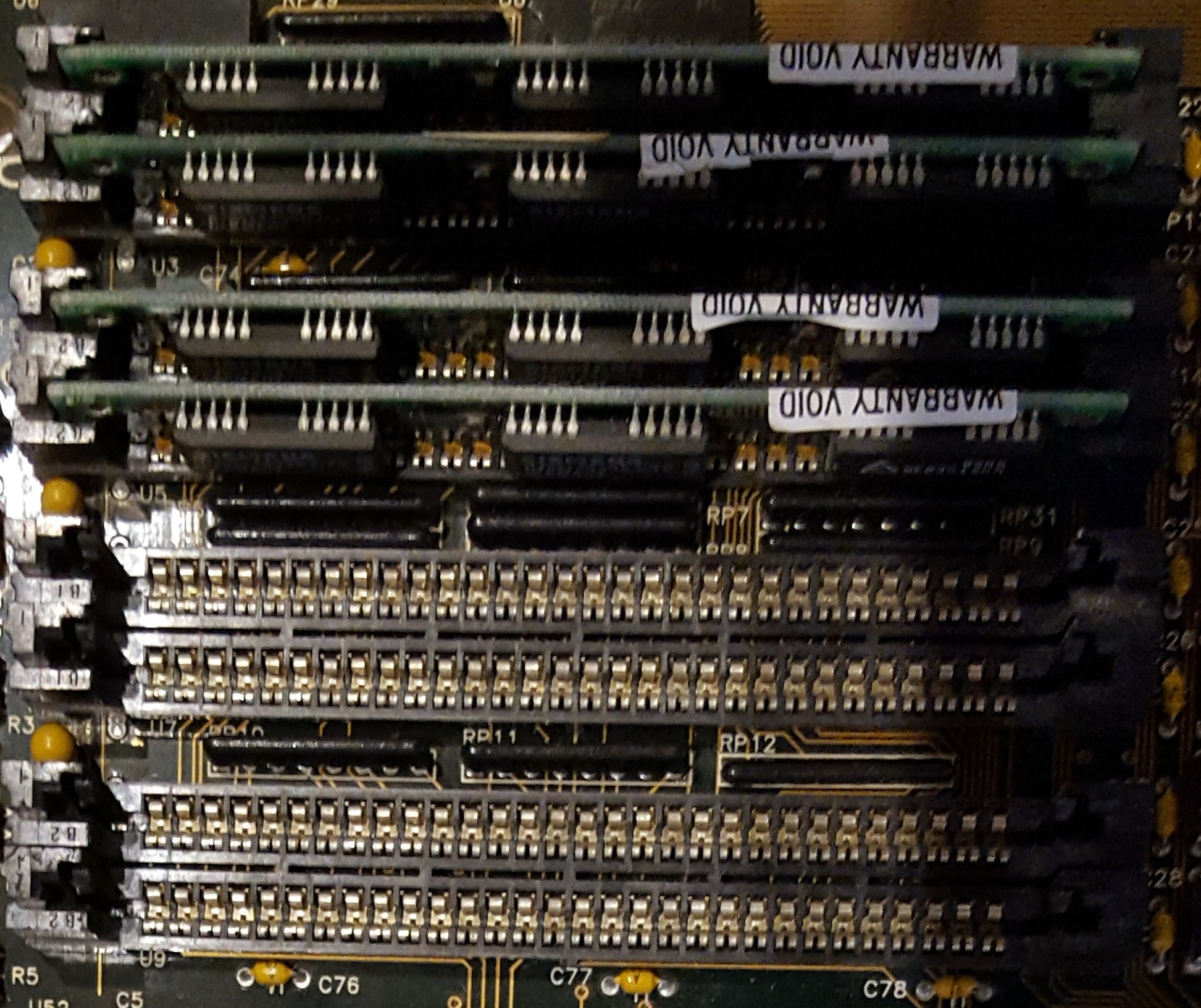
- Twelve 256 Kbit DRAMs for main memory, and two rows of holes above that could be for SIPP headers.
- Six 16-bit ISA expansion slots and two 8-bit.
- AT P8/P9 power connector
- Full-size DIN keyboard socket
Date-wise, the most recent date stamp on the motherboards' non-socketed chips is week 50 of 1988, so it was certainly no earlier than mid-December 1988 when this was originally manufactured.
The Component Parts
The CPU
 The 80286 CPU started off in clock speeds of 4, 6 and 8 MHz. Intel's versions of these later went up to 12.5 MHz, but authorised third parties like Harris Semiconductor managed to reach speeds of up to 25 MHz! So the 10 MHz variant I have here in Intel form was quite common for early 286 PCs.
80286s were always packaged in an "LCC" (Leadless Chip Carrier) package, either in Ceramic (CLCC) or plastic (PLCC) form. Rather than other ICs which have "leads" (pins), these have rounded pins underneath that compress when they go into the socket, supposedly to reduce the risk of bending a pin during insertion or extraction. They are still a real pain to get out of their socket, especially if they've been in there for 30 years! The best way to remove the CPU is to use a dedicated IC puller which comprises two prongs that fit into the two opposite corners. You can then pull up whilst rocking the CPU from side to side.
For this CPU, the external bus would also run at 10 MHz or possibly up to 12 MHz. There are three crystal oscillators on the board which are 8 MHz, 14.3 MHz, and 24 MHz. The latter is probably for the CPU, as boards at this time ran the CPU at CLK/2 - this may mean it's slightly overclocking the 10 MHz 286 to 12 MHz.
The Chipset
The chipset found on this board is the G2 GC101/102 PC/AT Chipset from February 1988. I see in some documentation that G2 is owned by Headland Technologies, so G2 must have been bought out at some point. The chips that make up this G2 chipset are as follows:
- GC101 - Peforms CPU and peripheral support functions including DMA controller, memory mapper, timers, counters, interrupt controllers, a bus controller, and all supporting circuitry.
- GC102 (x2) - Can be configured as either an address buffer or data buffer. Replaces address buffers, data trasceivers, memory drivers, parity generators and supporting circuitry.
I know of several commercially-sold PCs that used this GC101/102 chipset: The 80286-based Philips P2230, the Qualogy QPC-5132, the Tai-Hsin Group 286/EMS 286 and the Kouwell KW-241 286. The chipset is apparently available in either 12 MHz or 16 MHz versions (so as mentioned, it's possible my 10 MHz CPU is being slightly overclocked to 12), and supports up to 4 MB of memory using either 1 Mbit or 256 Kbit DRAM chips.
The BIOS, as we'll see in a bit, is essentially the same as the NEAT chipset found on my 386 C&T motherboard. And just like my review of that board, the AMI BIOS in this 286 was really not designed for consumer tweaking - it existed so that OEMs and third-party system builders could adjust the PC's performance to suit the specific hardware they were installing, such as the CPU, memory capacity, etc. The BIOS allows us to configure the CPU and AT bus's clock rates, as well as memory and I/O wait states and delays. DRAM type, shadow RAM capability and DMA wait states can also be programmed. The GC101 chip mentioned above is the one that also contains the CMOS RAM memory used to store the chipset configuration.
MEMORY
 The motherboard has twelve DRAM sockets, populated with 256 Kbit memory chips.
As I learned about this chipset, it supports a maximum of 4 MB of memory if 1 Mbit DRAM chips are used - this is very common even on high-end 80286 motherboards. Despite the fact that the 80286 can address up to 16 MB, motherboard support for a full 16 MB was quite rare. Since this board has 256 Kbit chips, it currently has 1 MB of memory onboard.
Strangely, 9 of the memory chips are 100ns and 3 are 120ns. This may cause problems when I attempt to get this board running at the fastest possible speed.
JUMPERS
The 286 motherboard has a number of jumpers and DIP switches which are setup as follows:
| Jumper | Setting | Location |
|---|---|---|
| W1 | 1-2 short | 1 wait state (set 2-3 short for 0 wait states) |
| W2 | 1-2 short | Unknown (silkscreen markings state 1-2 = A, 2-3 = B) |
| W6 | 1-2 short | BIOS = 27256 Kbits each (2-3 = 27128 Kbit chips) |
| W7 | open | Color/Mono (short = mono) |
| W9 | 1-2 short | Parity check (1-2 = enabled, 2-3 = disabled) |
| SW1-1 | off | Hi-speed |
| SW1-2 | on | I/O bus half speed |
| SW1-3 | off | RSEL0 |
| SW1-4 | off | RSEL1 |
Other test hardware
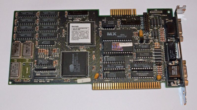
For video, I used my beloved Cirrus Logic CL-GD510/520 auto-switching Super VGA card. This card is only an 8-bit card but is auto-detecting so is a great solution for testing different video modes and monitors!

The Cirrus Logic CL-GD510/520 Super VGA video card with Eagle II BIOS
For testing I'm going to use an ATX 400W PSU from an old Pentium 4, coupled with an ATX-to-AT adapter. You can pick these adapters up inexpensively from various online stores and they come in very handy given the rarity of AT-style power supplies these days. Some varieties come with a power switch while others come with female blade connectors that must be shorted for power to be drawn.
POWER ON
Success! The board of course complains of a CMOS checksum failure, and has resorted to its static defaults due to having no backup battery.
At the bottom of the boot screen we see the BIOS boot string "ENET-1138-092588-K0" - The "E" in "ENET" means the BIOS has Extended Setup program. "NET" refers to "NEAT Chipset", the "1138" is American Megatrends' manufacturer reference number for Win-Win Computer, the "092588" is the BIOS date (25th September 1988), and "K0" is the AMI keyboard BIOS version number.
Slightly at odds with my original thinking is the reported memory: 1408 KB. We'll dig into that as we go through the BIOS in part 2.
